")
")
DEVICE DEVELOPMENTS
Photodetector elements (PDs) for the wavelength range of l = 1.3 - 1.55 µm
 | 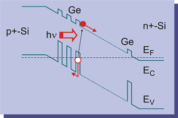 |  |
Aim: building-in (inclusion) in the complex of photon components of fiber-optical communication lines, including that based on one uniform silicon chip.
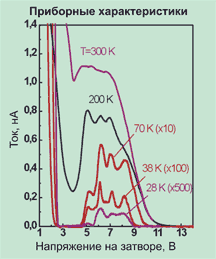
Description parameters: wavelength range — 1.3-1.55 µm, quantum efficiency — up to 21%, functioning t — room temperature.
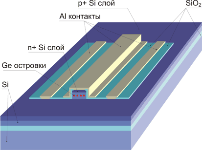
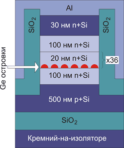
Technological bases: Ge/Si heterostructures with quantum dots MBE.
Field transistor on Ge/Si structures with quantum dots
 | 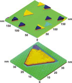 |
| automatic installation of MBE to synthesize multilayer semiconductor structures | Ge nanoclusters in Si: Ge islands density 3x1011 cm-2;lateral size 10-30 nm |
- The technology to obtain Ge quantum dots arrays in Si was developed
- A nanotransistor framework on the structures with Ge quantum dots in Si was created
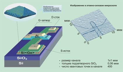
Framework of the field transistor with Ge QDs
Application:
- new quantum electron and optoelectron devices functioning at room temperature (electrometers, memory elements);
- element base of the XXI century's computing devices of higher rapidity.