")
")
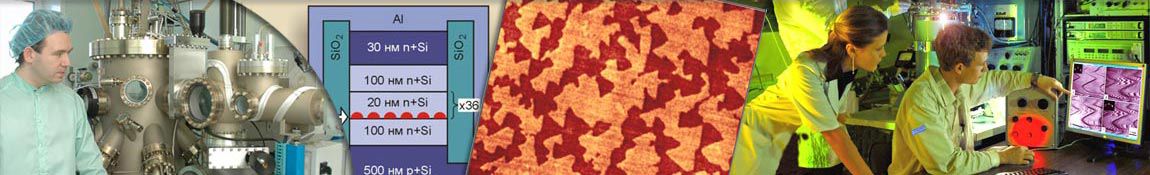


Aim:
building-in (inclusion) in the complex of photon components of fiber-optical communication lines, including that based on one uniform silicon chip.
Description parameters:
- wavelength range - 1.3-1.55 µm,
- quantum efficiency - to 21%,
- functioning t — room temperature.
Technological bases:
Ge/Si heterostructures with quantum dots MBE.


- Technology of fabrication of arrays of Ge quantum dots in Si was developed
- Nanotransistor with a layer of Ge quantum dots in a Si channel was produced
Application:
- New quantum electron and optoelectron devices functioning at room temperature (electrometers, memory elements),
- Element base of the XXI century's computing devices of higher rapidity.

A.Ioffe PTI, St.-Petersburg
Institut fuer Festkorperphysik and Center of NanoPhotonics Technische Universitat Berlin

Schematic illustration of parallel optical network based on VCSELs array (A), device layout (B) and microscope image of the developed VCSEL (C).
The development of the array configuration of such VCSELs can open the prospects for 1 Tbit/s optical network.
The A.V. Rzhanov institute of semiconductor physics SB RAS, A.Ioffe PTI, St.-Petersburg, Institut fuer Festkorperphysik and Center of NanoPhotonics Technische Universitat Berlin.

Characteristics
Parameters of tested SOI CMOS integral circuits (IC) based on 90 nm partially depleated SOI CMOS field effect transistors (FET’s) were investigated both theoretically and experimentally. Low values of threshold voltages (±0,6 V) were obtained by thinning of nitrided gate oxide up to 5 nm and isotype doping of poly- crystalline gates lied over highly doped n- and p-channels (~1018 сm-3) of transistors. As was shown at extreme condition of testing at increased temperatures up to 250°C and totaldose irradidation up to 50 Mrad all invertors have the same transfer characteristics, as at room temperature and all irradiated invertorsafter dose 10 Mrad also have trial characteristics as unirradiated ones keeping leakage current below 2×10⁻⁸ А.
Low shifts in characteristics of SOI
 |
| Fig.1. AFM image of 90 nm silicon gates CMOS IC’s even at more higher temperatures |
All technology is based on domestic technological equipment as well as on FET devices and SOI structures, developed in ISP SB RAS. Russian analogs are absent. All elements of IC’s are adapted not only to 90 nm but also to 1-2 mm technological nodes, which are common for the Russian industrial microelectronics plants.
Fields of applicationSOI CMOS IC’s are useable in extreme environment of high energy nuclear physics, geophysics, nuclear plant production, aviation and cosmic unperturbed telecommunication and transport systems, which can also be experienced with high thermal loadings.
SOI IC’s elements are developed, that applicable as well as for design of large and very large scale integration IC’s of SRH IC’s class and for commercial IC’s in automatic and control for high temperature parameters of fuel motors and power electric engines.
SOI production technology of ISP SB RAS is protected by 4 Russian patents and PCT invents. SOI CMOS FET’s design is based on the row of "know-how"s, which are not sent yet to the patent authorities.

|
||||||||||||||||


A brand-new semiconductor nanosystems structuring technology based on deep local anode oxidation of Ti GaAs ans Si surfaces with the conducting atom-voltaic microscope probe using additional potential was elaborated. This technology allowed us to master a principally new size scale in nanostructures fabrication (10 - 100 nm). A quantum interferometer, efficient radius 90 nm, was developed and produced. So small sizes allowed us to increase the interferometer functional temperature a level higher (to 15 K).
 |  |
 |  |
Topographical (a) and phase (b) images of AlGaAs/GaAs with a section of locally oxidised probe of atom-voltaic microscope (quantum interferometer) (c) - profile of relief along the red span AB. (d) Aaron Bohm interferometer oscillations. Oscillation period B = 0.16 T is adequate to efficient radius r = 90 nm.
Application field:
nanotechnology;
magnetic sensors.
Contact us:
Institute of Semiconductor Physics , 13 Ac. Lavrentyev Ave., 630090, Novosibirsk, Russian Federation, tel.: +7(383)333-10-80, fax: +7(383)333-27-71, e-mail:

| Aim: | Information transmition from the transmitter (Alice) to the detector (Bob) over optical connection line with absolute secrecy. |
| Problems: | 1. Classical transmission line with a big number of photons is not protected from eavesdropping. 2. Classical cryptography is based on the absence of rapid factorisation algorithm for big numbers. |
| Method: | Information carrier - single polarized photon |
| Base: | Laws of quantum mechanics - each measurement changes a photon quantum state. Spy (Eva) eavesdropping is connected with measurement and further reproduction (cloning) of a photon state. However, precise photon cloning is impossible! |

|
 | ||||||||||||||||||||||||


|
Coded phrase:
Greetings to the participants of the third seminar devoted to the memory of D.N. Klyshko!
Decoded phrase:
Greetings to the partivicipants of the third emi8nar devGot(ed to the memory of D.N. Klyshko!
Адрес:
Institute of Semiconductor Physics , 13 Ac. Lavrentyev Ave., 630090, Novosibirsk, Russian Federation, tel.: +7(383)333-24-08, e-mail:

The system of heteroepitaxial CdHgTe structures growth with MBE has been developed in the Institute.

 | Electron-optical transformers with semiconductor photocathods are being developed based on the scientific elaborations of ISP SB RAS, unique serial fabrication technology for EOD and super-vaccum serial equipment developed by "Cathod" OJSC that provides the forming functional nanolayers of semiconductor photocathods at the atomic level.
It is provided by:
| |
 | ||


1998 - 2008 - more than 5 th. SOI wafers, d=100 and 150 mm, were fabricated at the ISP experimental production line for micro- and nanoelectronic devices. Equipment worked out its output capacity. For a new line, it costs (200 mm, 5 th, it./yesr) - to 300 mln. roubles; (300 mm, 30 th it/year) - to 500 mln. r. Clean premises - 200 mln. r.


Micro- and nanochannel substrates of monocrystalline silicon may be used in the registration of big organic molecules and filtration of ultra-dispersive biological molecules and nanoparticles.
The optical microchannel DNA sensor is a silicon plate with channels sized 15 x 15 µm inside of which a certain number of oligonucleotide marker-probes (DNA fragments) dissipate. In light transmission through such a plate (wafer), IR absorption peaks are registered. If DNA molecules are added to the solution, they can be complementarily bound with marker-molecules immobilised on the plate. According to the change of IR absorption spectrum, it is possible to consider the presence of DNA hybridisation reaction (binding).
ISP SB RAS and ICBPM SB RAS Device Development


Description
- a physico-mathematical model and algorithms for 2D distribution simulation of basic avalanche physical parameters depending on major technological and topological device peculiarities were developed;
- framework variants of two types of discrete detectors - silicon pin-diodes and avalanche diodes with a laterally broadened pn-transition line;
- a technological route to fabricate discrete dtectors framework crystals (2-3 mnths - average time before fabrication) was worked out, and a variant of their installation in the corpus with external electrical outputs was developed;
- preliminary test methods were developed and perfected for both IR and gasodynamic trap in the Institute of Nuclear Physics, experimental data on detectors response to different types of ionizing radiations;
- methods to grow scintillational crystals to fit detectorts size were developed; variants of their conjugation with each other were approbed;
 |  |
| Cross-section of two detector elements | Crystals image of avalanche diodes line on a silicon wafer |
In the figure, a cross-section of the structure with 2 two cells of the LD line is presented. Particles penetrate the p+ external area into the depth which depends on particles energy. The range is about 100 µmfor protons with the energy 3.02 MeV. Appearance out of electron-hole pairs occurs during deceleration. Pairs are separated in the electric field and then they are registered.
Technical-economic advantages
High sensitivity of avalanche diodes to penetrating radiation is conditioned by the thing that, in them, charge carriers generated by light, passing through the p-n transition, acquire the energy in the strong electric transition filed (more than 105 V/cm) sufficient impact lattice atoms ionization and create secondary charge carriers on their way. As a result, a current signal increases many times by avalanche multiplication.
Fields of application
LDs are used as dtectors of penetrating radiations. In combination with scintillational crystals, such detectors are used both in experimental nuclear physics and particles physics, also positron emission tomography (including positron tomography of human cortex)

Description
The linear photoreceiver based on HES CdHgTe MBE, using MCSDP multiplexer
provides the following functioning regimes:
supply of positive polarity regulated back bias on photodiodes, readout of photodiode
signals using direct injection scheme, storage of these signals as charge packets, protection
from charge overflow for each photodiode, temporary delay and accumulation (TDA) for
each channel consisting of four photodiodes, two-directional TDA scanning, deselection
(turn off) of any photodiode if necessary, substitution of average background current
instead of deselected diodes, scheme control using consecutive and parallel interface,
changing integration time within broad limits with a simple external signal.
The basic parameters of linear photoreceiver 288x4 elements based on HES MBE for spectral atmospheric transperancy window of 8 -12чm are presented in the table:
|
 |  |
Fig. Topogram of linear photoreceiving module
288x4 specific detectability.
| Fig. Diodes photoresponse spectrum of
linear photoreceiving module 288x4
|
Technical-Economic Advantages
Using a linear PR in IR thermovision systems with image scanning allows to obtain
panoramic images of scanning angle up to 360°.
Moreover, the TDA regime for each channel consisting of four photodiodes allows to heighten specific detectability (D) twice compared to a matrix PR.
Fields of Application
Linear photoreceiving module is meant for furnishing IR thermovision systems
used in medicine, electroenergetics, terrestrial, air and aquatic transport, metallurgical, pharmaceutical productions and construction. IR thermovision systems
are aimed at objects detection on their thermal irradiation and also remote temperature
control of an object with high temperature (0.01 K) resolution.

Characteristics
Technology for reduction of resistivity deflection with temperature as well as for correction nominal values of power resistive elements was elaborated (in a cooperation with Joint Stock Company "NEVZ-SOYZ"). Resistors of tablet form were manufactured due to the use of neutron doped FZ silicon. Stabilized characteristic owing to high-energy irradiation was achieved by means of electrons or γ-rays and subsequent thermal treatments. Resistors with deflection of resistance within ±10% from nominal values in a range of temperatures +20÷+180°С. were created.

Technical and economic advantages
Powerful silicon resistors possess:
- High value of power-handling capacity for heat dissipation;
- Over-stability of nominal value resistance in operating temperature range;
- Low values of spurious inductance and capacitance;
- Opportunity for fine adjustment of nominal value of resistance.
Application area
The powerful silicon resistors of the tablet form will find wide application in power electronics. These resistors are optimal for application within unified cooling system with advanced powerful semiconductor devices: diodes, thyristors, IGBT-modules etc. It allows considerably improving both mass and geometric parameters of devices for commutation and control over power-consuming equipment.

Electrically reprogrammed and energy-independent memory (FLASH), alongside with random access memory and microprocessors, is predominant in silicon micro-circuits market. Since 2001 up to the present, within agreements with Samsung Electronics, physical principles of energy-independent terabit memory circuits have been investigated in the ISP SB RAS. New low-voltaic rapid-function memory elements with the use of insulators with high dielectric penetration (high-k dielectrics) were proposed.
 Memory element on charge localisation effect in amorphous silicon nitride |
 Memory element on electron localisation effect in silicon quantum dots |
 Characteristics of memory element reprogramming using SiO2 dots and high-k insulator Al2O3 (regular line) |
 Trap structure responsible for the memory effect in Si2N4 Si-Si connection of minimal silicon cluster |
A program simulation package was developed at the ISP in co-operation with IAE:
processes of charge transfer and localisation in amorphous insulators;
fill-in properties of enrgy-independent memory elements (record/erasure, data preservation);
optimization of terabit memory device construction
Contact us:
Institute of Semiconductor Physics , 13 Ac. Lavrentyev Ave., 630090, Novosibirsk, Russian Federation, tel.: +7(383)333-38-64, fax: +7(383)333-27-71, e-mail:
|
 |
| Silicon ingot parameters | Si-C | Si-FZ |
| Amount of electrically active background impurities, at/cm3 | <1x10¹² | <1x10¹² |
| Atom concentration at/cm3: -oxygen -carbon -heavy and alkali metals | 2-11x1017 <1x10¹⁶ <5x10¹² |
- <1x10¹⁶ 1x10¹² |
| Electric resistivity, ohm x cm | 0,05 - 200 | above 800 |
| Electric resistivity spread over ingot diameter, % | 3 - 5 | 3 |
| Ingot diameter, mm | 203 | 152 |
Commercial proposals:
supply of ground and polished silicon plates to suit customer's
specifications.

MAIN RESULTS:
The base MBE technology for multilayer semiconductor structures of In-Al-Ga-As compounds was developed.
"Heteroepitaxial structures of GaAlAs compounds" were developed and authorized - TA 1778-03533808-01 - on:
heteroepitaxial structures n+-GaAs/n-GaAs/GaAs for powerful MW transistors of MESFET type;
heteroepitaxial structures n+-GaAs/AlGaAs/n-GaAs/GaAs for powerful MW transistors of HFET type.
Based on these heterostructures OJSC "Oktava" (Novosibirsk) developed a number of MW modules.
 |  |
 | |

The technology of obtaining multilayer structures with the method of direct silicon wafer splicing (DSS) for developing the element base of voltaic intellectual microelectronics was developed.
 Thermovision image of two-layer structures | ADVANTAGES OF DSS TECHNOLOGY high reproduction of functional layer electrophysical parameters (use of FZ-Si); |
DSS structure provides the fabrication of finely precise (I=20-100A) vertical channel high-voltage transistors (U=1000-1700В) (MOS, LET, IGBT) and high rapidity diods with high output of quality products.
|  |
A series of transistors with static induction was produced on DSS structures by OJSC NEVP SOYUZ for voltage 800-1200V characterised by: low losses in the open state, high rapidity, higher radiation resistance.
Commercial proposals:
- serial production of DSS structures of type n--n+, n--p+, p--p+;
- working out the technology of vertical channel voltaic microelectronic device fabrication on DSS structures


"Katun" installation (device) with gas source of ammonia to grow nanoheterostructures based on GaN, AlGaN and AlN

 | Aim:
|
 |  |
| Control of quantum structures parameters | High-vaccum MBE Cd-Hg-Te installation equipped with high-speed laser ellipsometer |

 | Aim:
|
 |  |
| Ellipsometrical control during periodical nanostructures growth |

Spectroscopic Reflectometer KRS-200 is designed to measure the intensity of light scattering in transparent materials, such as crystals, glass, liquids in order to determine the concentration of scattering impurities, structural defects, foreign inclusions, etc. In addition, the reflectometer can be used as a spectrophotometer to determine the spectral transmittance and transparency boundaries of optical materials. Through the use of built- in polarizer one can measure the dichroism and determine birefringence in anisotropic materials.
Specifications
- spectral range .................................. 200÷1000nm;
- spectral resolution .............................. 2nm;
- cuvette dimensions ............................. 100×100×160mm;
- minimum dimensions of the sample .................... 5×5×15mm;
- maximum dimensions of the sample ................... 90×90×150mm;
- interface USB.
Flexible software designed for OS Windows 2000/XP provides control of the device in various modes of measurement, data acquisition, output of the measured spectra in numerical and graphical form, their further analysis and processing.

General view of the device.
Advantage
The domestic industry has not produced analytical equipment for research and analysis volume scattering of optical materials. In addition to a solution of this problems, the instrument allows us to determine the range of transparency, the availability and range of dichroism, other parameters, i.e implement a comprehensive quality control of optical materials.Application field
Optics, optoelectronics, quantum electronics, photonics, optical materials, as well as studies of scattering and turbid media.
Physical Bases of Integral Microphotoelectronics and 3D Nanostructures, and Physics and Technology Laboratory
Open Joint-Stock Company SIMEX

Fourier IR spectrometer "PT-801" and IR microscope "MICRAN"
Device production company:
Open Joint-Stock Company SIMEX - scientific-production enterprise - winner of the "Golden Mercury" competition in the nomination "Best small innovative enterprise - 2008", Novosibirsk.
ISP SB RAS device developers:
Scientific-Technological Department; Fourier Spectrometry Group; Physical Bases of Integral Microphotoelectronics and 3D Nanostructures, and Physics and Technology Laboratory.

Description
The stand-imitator (fig.) is aimed at the terrestrial imitation of the technological zone in space behind the protective molecular screen and at the check of technologhical elements efficiency, their testing, tuning and graduation, also at working out cyclograms and algorithms of technological processes to obtain multilayer semiconductor nanostructures under the conditions of ISC flight. The stand has a vacuum chamber (1) in which a container with a drum mechanism is inloaded (2) to heat and fix the wafers 100 mm in diameter. The chamber has a prelimnary pumping block, NMD-04 pumps, sublimation pump that consists of a cryopanel with a system of liquid nitrogen transport and a sublimator. Hermeticity of flanged joints is provided by copper and vitonum spacers. Control of environmental parameters (1) is realised by means of the pressure sensor and mass-spectrometer (not shown); control of the films being grown - by the diffractometer (5) with a luminiscent screen (6) and a laser ellipsometer (7).
Automatic control of the technological process, when carrying out the experiment of thin-film growth, is realised by the control block (3) which provides the: installation of the chosen wafer in a technological position, heating the wafer, heater temperature measurement, control of the wafer shutter, control of sources working regimes in growing epitaxial structures and that of molecular sources shutters (MS). When implementing a technological process, MS shuters open and MS materials heated in crucibles form molecular beams interacting with the wafer surface; it provides the growth of semiconductor nanostructures on its surface with set layers thicknesses and a certain chemical composition. Control of structures quality is realised according to the diffraction image obtained on the luminiscent screen (6) as a result of electron beam reflection (going out of the diffractometer cannon (5) from the wafer surface. Another control method is ellipsometry that allows us to monitor epitaxial films composition and growth.
 |
| Fig. Stand-imitator with installed nodes and VMD MBE elements ready for LT. 1-chamber of the stand-imitator, 2. drum mechanism, 3. electron devices to control the technological process, 4. head computer, HEED electron cannon, HEED fluorescent screen, optical ellipsometric arms, 8. molecular sources. |
Technical-economic advantages
''Epicenter'', the cosmic vacuum stand-imitator can be used as an MBE installation, also for mastering nanotechnologies and training young spacialists under plant conditions and university nanotechnological centers. In this version, it has the following big advantages compared to all known analogues:
- compact size;
- экономичность по расходу жидкого азота и исходных особо-чистых материалов;
- economical use of nitrogen and initial ultra-pure materials;
- high precision of program maintenance of temperature sources and wafers;
- precisional control of synthesised films structural state and thickness.

Description
System depending on directions of its use can consist of several specialized
vacuum chambers: chamber of loading-unloading of wafers-substrates with a cassette (2
cartridges on 7 plates of 102 mm in diameter); a chamber for epitaxial growth of
elementary semiconductors (Si, Ge), metal, dielectric layers are supplied with electron
beam evaporators, gas and plasma sources; chambers for growth of A3B5, A3N and A2B6
semiconductor compounds can contain 12 molecular sources, including the valve type for
antimony, phosphorus, arsenic etc. All chambers are rigged by high-energy electron
diffractometers developed and made in the ISP, Siberian Branch of the Russian Academy
of Sciences and an automatic laser ellipsometer - devices for not destroying control of
structure and properties of produced nanogeterostuctures in the course of their synthesis.
The combination of working chambers in any order is possible. Transport of substrates
between working chambers is automated. The installation rigged by the computer control
system and the software package for processes was carried out. Film growth rates are
average from an atomic layer to micrometers an hour.
In a set with installation or separately, the following units can be delivered:
- crucibles from pyrolitic nitride of various sizes, processed by an original technique according to demands of epitaxial production engineering;
- crucible, valve-type and electron beam sources of molecular beams;
- high-energy electron diffractometers (speeding up voltage to 30 kV) with the system for registration of a diffraction pattern and the analysis of their intensity with the software;
- automatic laser ellipsometer for registration of optical, morphological, magnetic parameters and the thickness of thin-film structures in the course of their growth and after;
- optical pyrometers;
- power modules and computer control systems with the software.

A two-chamber variant of "Katun-100" on an assembly section in the A.V.Rzhanov Institute of Semiconductor Physics, Siberian Branch of the Russian Academy of Sciences.
Technical and economic advantages
- compactness, low cost and profitability;
- novelty and originality of technological solutions (are protected by patents and a know-how);
- economy of materials and high characteristics of epitaxial structures at the low cost price of a process;
- automatic loading-unloading of wafers-substrates;
- absence of magnetic manipulators and the variable magnetic fields connected with them;
- the automated control system of a process completed with power modules and system of the exact thermoregulation, supplied with the original software, allows us to realize the processes in the automatic regime;
- convenience both for University Laboratory and for industrial use.
Application fields
Conducting experimental researches and the industrially-oriented work- outs in
the field of physics of the condensed condition and synthesis of semi-conductor and metal
nanostructures. Training specialists in the field of nanotechnology. Manufacture of
multilayered heteroepitaxial structures is meant for the element base of micro - nano - and
optronics, microwave devices, photovoltaic, light-emission and photosensitive devices,
navigating equipment, laser and telecommunication systems, satellite television, etc.

Institute of Chemical Biology and Fundamental Medicine, SB RAS.
Description
The polarization-optical DNA sensor provides optimal conditions for detecting of
complimentary complexes formation processes with immobilized oligonucleotides on a carrier body surface with DNA chips.
DNA sensor provides increased
reliability of the analysis, increase in
sensitivity and operating speed.
The software is created for DNA sensor control including the block of graphical representation of the information in the compressed window, providing sensor operation, reception and processing of the information and representation to its user in a convenient aspect.
The diagram processing is applied with the purpose of increasing detectability of a sensor. Fifty one-dimensional files are allocated in the program under logged data.
Accuracy of the sensing transducer positioning - 1 micron in DNA chip analysis.

DNA Sensor

Description
Strain gage transducer designed for detection of the lateral rock deformation in
relief holes with small-scale diameter (80-85 or 115-120 mm) in three directions by
means of polarization-sensitive pickups shifted off 120 degrees. The measurements of
the mechanical strength, raised in rock is based on the method of the high accuracy
detecting of linear changes in relief hole geometrical sizes. Polarization-sensitive pickups detect the deformation in three directions and that allows on-line monitoring the
shearing of load-carrying frame, rock bursts, earthquakes, and technogeneous dangerous works.
| Temperature instability, degrees; | 4×10⁻⁷ |
| Range of output linear characteristic; | 103 |
| Power supply, V; | +5 |
| Power consumption, mW, below | 65 |

Technical and Economic Advantages
High sensitivity of sensing transducers, more than in 50 times surpassing in
sensitivity strain-gauge transducers of other types. Design allowed the recurrence of the
application, the simplified installation. It is supposed more than thirtyfold over loadings
on a dynamic range. A problem of the temperature stabilization of the polarization-sensitive
pickups is solved.
Area of Applications
Mineral industry, metallurgy, construction, carrying out the tasks of the Ministry
of Emergent Situations of the Russian Federation.

Description
Tension metric station having a set from 1 to 8 high sensitive mini sensors intended
for the analysis of distribution of deformations in the block constructions is constructed.
The sensors (based on the application of photo-elastic effect) show the sensor sensitivity
50 times more when compared to the tension metric sensors based on film resistors (Tension
sensor base - 15 mm; Sensitivity to changes of comparative deformation - 1×10⁻⁷;
Temperature instability - 4×10⁻⁷ Deg.; Sensor interrogation period not more - 10 ms).
Technical and Economical Advantages:
- Multiple applications,
- Simple (reductive) assembling,
- Absence of glue joints.
- 30 times dynamic over loading ranges are possible.
Application Areas:
- Mechanical engineering,
- Mining industry,
- Metallurgy,
- Building industry.

Science and Engineering Co. "TORI", Ltd.
General characteristic
Multifunctional System for Pipeline Monitoring is intended for registration of out-flowes, guarding of pipelines. The system is applied to an ultra-long acoustic loca- tion of shells, and also provides a number of subfunctions for technical diagnostic of oil, products and gas pipelines.

The outcome data are summarized graphically on the operator PC display. Those data are transmitted to the remote computer for process inspection. The coordination with the technology card, interception of natural barriers and high-altitude situation of the pipeline above the sea level are realized at the actual time scale. The scaling of cards allows receiving more detailed coordination.
The system consists of 4 modules: acoustic antennas-1, controllers-2, a system control computer -3 and software-4. The modules 1 and 2 are installed on a linear part of a pipeline. The computer is arranged, as a rule, at the dispatching office of the pipeline. The structural diagram of the system is shown at the Figure.
Technological and economical advantages
The technological and economic advantages are reached due to the following factors:
Multifunctionality and, therefore, capability to replace various types of equipment;
Decrease of product losses resulting by the emergency outflows, unauthorized insets and thefts during the transfer;
No need for tracking all shells by mobile crew, the manager can do all necessary operations using PC software displaying the product transport on PC at real time regime;
No need for looking up for shells in case they have stopped;
Capability for operating control over shell transport to eliminate emergency shut-downs and clipping of shells;
Built-in hardware-software is available for the system operation monitoring, reduces the costs of service.
Fields of application
The system is applied on oil, products and gas pipelines.
The series production of a system is organized.
The separate clusters of a system are licensed.

Photodetectors (PD) are designed for carrying out astrophysical investigations on board a space vehicle with the aim of detecting lightly heated objects in space
 Photodetector | PD Construction:
|
|
| |||||||||||||||||||||


Commercial proposals:
- PD manufacturing (execution of an order - no longer than 6 months);
- supplying production equipment for fabrication of photosensitive layers;
- transferring the technology for manufacturing photosensitive layers

Programed power supplies "Impulse" of 1.25 or to 2.5 kW with an analogous external or manual control, connected to ECM, are meant to supply different devices with a possibility of programed regulation of objects regimes including the use of feedback channels. They provide stable voltage or stabilized current of from-zero-to-maximum regulation, have low pulsation level and high efficiency. It is possible to set output voltage of a special form (meander, triangle, saw, sinus) with a through-zero transition. The output of supplies is isolated. A connection to the general insulator of any output is permissible in external circuits.

Fig. Image of "Impulse" power supply.
Specification
- wide range of output voltages (6 - 200) and currents (to 100 A),
- active correction of power coefficient,
- automatic maintenance of set voltage and current,
- rough and precise setting of parameters with one handle through pressing,
- protection from short circuit of load circuit with self-regeneration,
- even voltage on-growth on the load in all regimes,
- saving the last setting,
- fan's noiseless rotation at small power on the load,
- dimensions — mm/weight, kg:
- 88×142×400/ 3,5 (до 1250 VA)
- 88×284×400/ 5,9 (до 2500 VA)
Technical-economic advantages
- compaction, high specific power,
- convenient for composition,
- multi-functionality.
Application fields
- testing, measuring and technological equipment,
- automatic control systems,
- equipment for testing and production of semiconductor devices.

Controller device "Technologist 2" is meant to control technological processes of laboratory and industrial installations. It is designed as 3U crate to be installed into frame 19". The necessary modules are mounted in the crate on the back side. In front is the panel with organs of indication and control. The controller is furnished by communication modules to be connected with ECM, precisional temperature regulation, spacing drive, ADC-DAC, discreet in- and outputs according to technical requirements for monitoring of technological process and the structure of control system.
Controllers software provides with the realisation of autonomous control of technological process by means of an intuitively clear button control desk with a two-line liquid crystal indicator, and also connection with ECM through USB interface - the upper level service. Functions that improve reliability and increase capability for technological installations with a long-time control cycle are realized in the software.

Fig. Fragment of a chamber with controllers.
Specification
- maximal amount of modules in the crate - 12 (+ 1 communication module),
- possibility of growing craters onto one communication line,
- temperature and temporal drift of temperature regulators < 1 μV on thermopair input;
- dimensions, mm - 132 × 484 × 330,
- weight - 8 kg.
Technical-economic advantages
- has no analogs for making up multichannel precisional temperature regulation systems,
- high reliability and universality.
Application fields
- testing, measuring and technological equipment,
- automatic control systems,
- equipment for testing and production of semiconductor devices.

All material bodies with the temperature higher than 0 K (-273 C) have electromagnetic radiation which, according to Planck law, looks curve-shaped with a maximum. The number of emitted radiation quants increases with an increase of an object's temperature. Objects thermal image is formed with a special IR objective and registered assisted with a radiation sensor installed in a lens focal plane. The radiation sensor is a hybrid integrated circuit installed on the cooled pedestal of the cryostat. The matrix elements transform light quants into electric charges which are accumulated in the near-surface n-IAs layer under the capacitor gate, red out by the silicon multiplexor, amplified, preliminarily processed by the electron circuit and transmitted in the computer. Image visualization can be made using the thing that the value of output signal from sensors is proportional to an object's temperature. Having obtained a 2D array of signal values from an object it is possible to get a black-and-white or color thermogram image. The minimal signal may be designated in black or violet color, the maximal — white or red. The intermediary values can be evenly distributed over 256 gradations of grey or color shades. Two device modifications, which differ in their spectral range, were fabricated (Fig. 1). IR lenses with optical 8- and 20-fold magnitude are used in the devices. The device spatial resolution at the signal intensity differentiation of 4% was equal to 1.6 mcm. The microscope's observation field depends on the used lens and the distance from it to the photodetector device (PDD).
 | Fig. 1. General view of IR scanning microscope: 1 — thermoimaging camera, 2 -stand, 3 — co-ordinate table, 3 — position sensor, 5- step engine of co- ordinate X, 6 — electron circuit of observed object positioning control. |
Basic device specification
| Spectral range | 2.6 — 3.05 mcm: |
| Matrix InAs-based PDD of dimensionality | 128×128 elements. |
| Element size | 40×40 mcm, step 50 mcm. |
| Frame frequency | 100 Hz. |
| Microscope observation field | from 420×420 to 1000×1000mcm. |
| Spectral range | 3-5 mcm: |
| Line InSb-based PDD | 192×2 elements. |
| Element size 40×40 mcm, step | 50 mcm; line elements are in two rows shifted releted to each other at 0.5 step. |
| Frame frequency | 5000 Hz. |
| Microscope observation field | from 625×4.8 to 1500×12 mcm. |
| Maximal scanning field is equal to | 100×50 mm. |
| NEYD | = 25 mK. |
| Measured temperatures range | from 15 °C to 150 °C. |

Fig. 2. View through the silicon commutator. Compatibility precision control in hybrid modules assembly on In microcolumns. Module size — 6.5×10.5 mm, image dimensionality — 3380×2000 pics, spatial resolution — 3.25 cm. A magnified image fragment is shown in the window.
Technical-economic advantage
IR microscopy is a unique instrument in studying thermal processes that proceed on microscopic scales and is a non-destructive investigation method for thermal processes.
Application fields
It can be used in the investigation of:- temperature processes that proceed on thin films surface;
- thermal radiation distribution on catalizers surface;
- thermal radiation distribution on sorbents surface;
- distribution of radiation emission from IR light diodes surface;
- temperature fields on visible range light diodes surface;
- heat distribution in voltaic elements of microelectronics;
- revealing defects in hybrid integrated PDD circuits assemblies.

Specification
The VEC is designed for investigating thin films structures within a wide temperature range, as well as adsorption/desorption processes, owing to the interaction of an atomic clean surface with the gaseous phase. The Complex consists of ultrafast laser ellipsometer mounted on the vacuum chamber equipped with a pumping system, lapping gases and thermocontrol.
| Basics specification | |
| Two-stage pumping system, residual pressure, no worse | 10-7 Torr |
| Possibility of inert gases | able |
| Temperature range | 20 - 500°С |
| Source wavelength | 633 nm |
| Accuracy in determining the Mueller matrix elements, no worse | 0,002 |
| Single measurement of ellipsometric parameters | 1 ms |
| Light spot, max | 3 mm |
| Dimensions | 800×900×1200 mm |
| Weight, max | 140 kg |
| Supply | 220-240 V/50Hz. |
General view of the instrument

Advantages
The developed instrument allows one to carry out ellipsometric measurements in vacuum or in inert gases that widen the range of applied and research tasks. The built-in heater makes it possible to perform fast-running temperature-dependent and temperature- induced processes. High performance of the instrument and user-friendly software allows you to collect and process a large volume of information and display it in real time So far such equipment is not produced in home and foreign industries.
Application fields
Scientific institutions, universities, as well as company-producers dealing with research tasks in the field of advanced materials for nanotechnology, solar cells, porous film structures, nonlinear optics, crystal physics, geochemistry, bionanotechnology, etc.