|
|
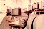
The history of the laboratory сis connected with the research developments in the field of radiation solid physics. At the end of 60's of the last century, at the ISP Laboratory of Radiation Physics, intensive research was carried out regarding physical phenomena under ion implantation, rapid electron and neutron radiation. The ion implantation method suggested in 1954 had a long list of potential advantages, whose realisation was delayed for a long time due to the problem in anihilation of defects that appear during accelerated electrons transmission in crystals. When searching new approaches in 1974, it was found that laser radiation nanosecond impulsive impact — at power density 107W/cm2 - on ion-doped semiconductor wafers with an amorphous layer leads to the crystal structure restoration. Transformation of an amorphous layer into a monocrystal at a huge speed (1-10 m/s) was an intriguing phenomenon that arouse the interest of researchers in different fields to laser anealing. To investigate the phenomenon of impulse-oriented crystalisation and doping processes, the Laboratory of Impulse Effects was organised at the ISP in 1984 (first as an interinstitutional laboratory Academy of Sci. and Ministry of Electron Industry). Its task was investigation the processes of crystals genesis under deep overcooling, doping elements solubility at high crystalisation rates, crystalisation on nonoriented wafers. A big progress was made in the solution of important microelectronic problems, i.e. obtaining thin doped semiconductor layers (for electric contacts, source/drain areas in field transistors) semiconductor films crystalisation on amorphous dielectric wafers. First of all, rapid thermal anealing systems based on the impact of light impulses of second and millisecond ranges became to be widely used in practice. At present, short- time impulse lasers find their application for silicon films crystallisation on glasses and for fabrication of matrices of thin-film transistors used to control liquid-crystalline displays
Also in the 70's of the last century, two basic modern methods of epitaxial growth were developed for the precisional control of thickness, planarity and composition. These are MB and gas-phase methods of epitaxy from metal-organic compounds. MBE method has become one of the most important technologies to grow quantum-dimensional structures. In 1987, the laboratory of impulse effects was offered to join the activities in MBE with the addition of radiation physics methods: ion implantation and laser anealing. The basic trend was in the synthesis and studies of nanostructures with QDs. The correction of the scientific trend lead to a change of the laboratory's name. A circle of problems in making nanostrctures with QDs now consists in: 1) the increase of QDs array homogeneity on sizes with the preservation of their uniform shape and element composition, 2) control of QDs spatial location (spatially ordered arrays), their density with a possibility to obtain extremely dense and discharged arrays, 3)decrease of defects density — dislocations and dots in QD nanostructures.
One of the successful approaches for the increase of homogeneity of QDs ensemble has become the method of impulse ion impact during epitaxy from molecular beams. Another approach is laser anealing of the grown structures, which allowed us to decrease the dispersion on quantum dots sizes in MBE-grown nanostructures.
A charge transfer over localised states of a non-ordered system is characterised by the tunnel mechanism in which the coulomb interaction can change the temperature dependence of a systems conductivity (from Mott law to Shklovsky-Efros dependence). Polarons formation is another effect of coulomb correlations. When a QD ensemble interacts with electromagnetic radiation (absorption of radiation), the oscillating charge density, on each quantum dot during transition, causes the appearance of a temporally and harmonically changing long-distance coulomb potential which affects the motion of all electrons. Such an electron-electron interaction manifests itself in the absorption spectrum as a band narrowing, increase of amplitude and a shift of the maximum to the high frequency area (depolarization effect).
Effects of interaction and disorder in QD nanostructures are also connected with elastic deformations that appear due to differences in constant lattices of QDs material and the matrix which quantum dots build in. In a dense array, there may be a supesition of elastic deformations fields from the neighbouring nanocrystals. It leads to a considerable change of a nanosystem's electron properties.
In the technology nanochanel membranes fabrication with profile and ordered nanochanels, and in the creation of devices on their base using one common approach using only silicon, it is supposed to produce nanofluid filters of the whole nanometer range and nanofilters which allow us to separate and concentrate ultradispersed nonorganic and biological agents. The profile structure of membranes with internal cavities will allow us to use them in creating solid optical active media with high semiconductor quantum dots concentration, e.g. CdS nanoparticles sized 1-10 nm. Based on the devices being developed, it will be possible to realise the process of separating biological molecules on their size and shape with further obtaining ultrapure, sterile concentrates for molecular biology and medical diagnostics.
|


|


